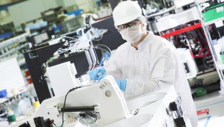
To fortify its global manufacturing and R&D capabilities, Applied Materials recently unveiled a multi-faceted plan to expand its operations in Singapore over the next eight years. Dubbed “Singapore 2030” the plan includes broadening its technology ecosystem partners in the city and developing the local workforce.

As part of Singapore 2030, the company held recently ground-breaking for the expansion of its regional hub in the city, which is home to Applied Materials’ largest factory outside of the United States. This investment of hundreds of millions of U.S. dollars will strengthen the company’s ability to meet growing customer demand in the years ahead.
“For the past 30 years, Singapore has been a strategic hub for Applied Materials, and we are excited to build on our success with new investments that will strengthen our ability to support the semiconductor industry on its path to becoming a US$1 trillion market by the end of the decade.”
Gary Dickerson, president and CEO of Applied Materials
He added: “We look forward to working with the Government of Singapore and the vibrant technology ecosystem to create opportunities for mutual growth that will benefit the global semiconductor industry.”
With the semiconductor industry entering a new wave of growth fuelled by the digital transformation of the economy, Applied Materials has revealed plans to make multi-billion-dollar investments in its innovation infrastructure in the United States and expand its global manufacturing capacity.
The company expanded to Singapore in 1991 with a small sales and service site that has grown to become a major manufacturing and regional operations hub with a workforce of more than 2,500. In 2019, it received the Distinguished Partner in Progress Award from the Government of Singapore in recognition of the company’s outstanding contributions and commitment to the city.
Bolstering R&D capability in Singapore

Furthermore, the company will invest to bolster its R&D capabilities in Singapore with a focus on accelerating the commercialisation of new technologies and services that improve chip power, performance, area, cost and time-to-market (PPACt™).
One example is the research collaboration between Applied and the Institute of Microelectronics (IME), a research institute of Singapore’s Agency for Science, Technology and Research (A*STAR), focused on hybrid bonding and other emerging, 3D chip integration technologies.
“Applied Materials is a longstanding partner for Singapore in advancing manufacturing and innovation in our semiconductor equipment industry. We strongly welcome the company’s ‘Singapore 2030’ plan, which will deepen Singapore’s role as a critical node in the global semiconductor supply chain,” said Beh Swan Gin, chairman of Singapore’s Economic Development Board.
Nurturing the local workforce
As a top employer, Applied will help enable a future-ready workforce for Singapore’s semiconductor equipment industry through enhanced training and advanced education programs. This includes an initiative with the Singapore Institute of Technology where Applied employees gain access to tailored learning modules in areas including AI and machine learning, smart manufacturing, robotics and automation, data science, and more.

“Applied Materials is committed to helping Singapore cultivate the workforce of tomorrow as digitalisation accelerates and technology becomes more important to the economy than ever before,” said Brian Tan, regional president, Applied Materials South East Asia.
He added: “Over the next several years, we plan to invest in new initiatives with our academic and community partners with an aim to deliver further value to Applied, to our customers, and to Singapore.”


